The article in English follows the Japanese version.
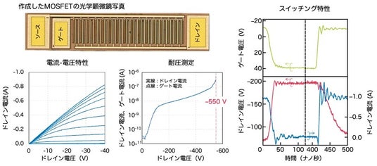
株式会社Power Diamond Systems(本社:東京都、代表取締役CEO:藤嶌 辰也)は、独自に開発を進めてきたダイヤモンドMOSFET技術を高度化し、ダイヤモンドデバイスとして世界で初めて、1つのデバイスにおいて耐圧550V、ドレイン電流0.8Aを実現しました。さらに、その同一デバイスを用いて、200V・1Aのスイッチング動作を達成し、世界最高水準の性能を実証しました。本成果は、ダイヤモンド半導体を用いたパワーデバイスの実用化に向けた重要な技術的マイルストーンとなるものです。
研究開発の背景
ダイヤモンド半導体は、ワイドバンドギャップや高い絶縁破壊電界、優れた熱伝導率などトップクラスの物性値を有しており、既存のシリコンやSiC、GaNを凌駕する次世代パワーデバイス材料として期待されています。その優れた特性から、次世代パワーエレクトロニクスを支える基盤材料として世界的な注目が高まっています。その実用化に向けて、高耐圧化と低オン抵抗化の両立が重要な技術課題となっていました。特に、高耐圧化の観点では、ゲート端部における電界集中によりドレイン・ソース間耐圧が制限されるという問題がありました。また、大電流とスイッチング評価に必要な特性の両立には1デバイスあたりの有効面積を抑え、小型デバイスを多数並列接続する必要がありました。
今回の研究開発成果
今回、Power Diamond Systemsがこれまで培ってきたダイヤモンドMOSFETの基盤技術をもとに、フィールドプレート構造を導入することでゲート端部における電界集中を抑制し、高耐圧化を達成しました。同時にデバイスの大面積化を進めることで高電流動作を可能とし、従来課題であった小型デバイスの並列接続に依存しない大電流駆動を実現しました。その結果、1つのダイヤモンドMOSFETにおいて素子耐圧550Vと0.8Aの電流を両立することに成功しました。これは、フィールドプレートを含むPower Diamond Systemsのデバイス設計およびプロセス技術のノウハウの有効性を実証する成果になりました。
また、同一デバイスを用いて、ダイヤモンドMOSFETとして世界で初めて200V・1Aのスイッチング動作を達成しました。本成果は、ダイヤモンドパワーデバイスが静特性評価の段階から実用動作検証の段階へと進展したことを示す成果になります。
Power Diamond Systemsは、安定したプロセスの確立により、再現性良くデバイスを作製できる環境を整えており、技術の安定性と実用化に向けた着実な進展を示しています。
今後は、ダイヤモンド半導体デバイスの社会実装に向け、国内外の研究機関、企業等の外部パートナーとの連携を通じ、さらなる技術開発、アプリケーション開発をより一層強化していきます。
なお、本研究成果は、2026年2月24日付でApplied Physics Express*に受理され、オンラインで掲載されました。
本研究成果の一部は、NEDO(国立研究開発法人新エネルギー・産業技術総合開発機構)の委託業務(JPNP14004)および文部科学省「マテリアル先端リサーチインフラ」事業の支援により得られたものです。
* Applied Physics Express
Field plate multi-finger diamond MOSFET with ampere-class current capability and breakdown voltage of 550 V
S. Shoji1, N. Oi1, S. Kawai1,3, R. Yoshida1,2, K. Ota1,2, A. Watanabe3, I. Omura3, K. Ueda2 and T. Fujishima1
1 Power Diamond Systems Inc., Shinjuku-ku, Tokyo 169-0051, Japan,
2 Waseda University, Wakamatsu-ku, Kitakyushu, Fukuoka 808-0135, Japan
3 Kyushu Institute of Technology, Wakamatsu-ku, Kitakyushu, Fukuoka 808-0196, Japan
株式会社Power Diamond Systems 事業概要
Power Diamond Systemsは、ダイヤモンド半導体デバイスの研究開発を行うスタートアップです。ダイヤモンド半導体デバイスは、モビリティ、再エネなどの次世代パワーエレクトロ二クス分野において期待される次世代パワー半導体です。このダイヤモンド半導体デバイスにより超小型・高効率インバータモジュールを実現し、エネルギー社会における更なる省エネ化に貢献することを目指しています。
会社名:株式会社Power Diamond Systems
所在地:東京都新宿区西早稲田1-22-3
早稲田大学アントレプレナーシップセンター
代表者:藤嶌 辰也
ホームページ:https://www.powerdiamondsys.com/
本件に関するお問い合わせ先
株式会社Power Diamond Systems 管理担当:高橋
Mail:[email protected]
Diamond MOSFET Demonstrates World’s First 200V/1A Switching Operation
- Achieves 550 V Breakdown Voltage and 0.8 A Current,
Accelerating the Deployment of Next-Generation Power Devices -
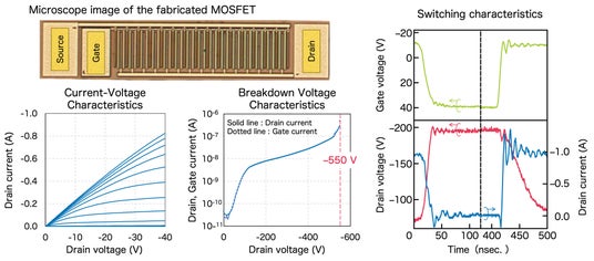
Power Diamond Systems, Inc. (Headquarters: Tokyo, Japan; CEO: Tatsuya Fujishima) has further advanced its proprietary diamond MOSFET technology and, for the first time in the world for a diamond-based device, achieved a breakdown voltage of 550 V and a drain current of 0.8 A in a single device. Furthermore, using the same device, the company successfully demonstrated 200 V / 1 A switching operation, establishing performance at the highest level reported to date. This achievement represents an important technological milestone toward the practical implementation of diamond semiconductor power devices.
Background of the Research
Diamond semiconductors possess outstanding material properties, including a wide bandgap, an extremely high dielectric breakdown field, and exceptional thermal conductivity, making them a promising next-generation power device material that could surpass conventional semiconductors such as silicon (Si), silicon carbide (SiC), and gallium nitride (GaN). Owing to these superior characteristics, diamond has attracted increasing global attention as a foundational material for next-generation power electronics. For practical implementation, however, achieving both high breakdown voltage and low on-resistance has remained a key technological challenge. In particular, from the standpoint of improving breakdown voltage, the concentration of the electric field at the gate edge has limited the drain-source breakdown voltage. In addition, realizing both high current capability and switching characteristics required for device evaluation necessitates reducing the effective area of each device and connecting a large number of small devices in parallel.
Research Results
In this study, Power Diamond Systems advanced its diamond MOSFET platform technology developed to date by introducing a field-plate structure, which suppresses electric field concentration at the gate edge and enables higher breakdown voltage. At the same time, the device area was increased to enable high-current operation, thereby achieving large-current driving without relying on the parallel connection of many small devices, which had been a limitation in previous approaches.
As a result, a single diamond MOSFET successfully achieved both a device breakdown voltage of 550 V and a drain current of 0.8 A. This result demonstrates the effectiveness of Power Diamond Systems’ device design and process technologies, including the implementation of the field-plate structure.
Furthermore, using the same device, the team achieved 200 V / 1 A switching operation, the first demonstration of such performance in a diamond MOSFET worldwide. This achievement indicates that diamond power devices have progressed from the stage of static characteristic evaluation to verification of practical switching operation.
Power Diamond Systems has also established a stable fabrication process that enables the reproducible production of devices, demonstrating both the reliability of the technology and steady progress toward practical implementation.
Looking ahead, the company will further strengthen technology development and application development through collaboration with research institutions and industry partners in Japan and overseas, with the aim of accelerating the societal implementation of diamond semiconductor devices.
This research was accepted for publication in Applied Physics Express* on February 24, 2026, and has been published online.
Part of this work was supported by a commissioned project from NEDO (New Energy and Industrial Technology Development Organization) (Project No. JPNP14004) and by the “Advanced Research Infrastructure for Materials and Nanotechnology in Japan” program of the Ministry of Education, Culture, Sports, Science and Technology (MEXT).
* Applied Physics Express
Field plate multi-finger diamond MOSFET with ampere-class current capability and breakdown voltage of 550 V
S. Shoji1, N. Oi1, S. Kawai1,3, R. Yoshida1,2, K. Ota1,2, A. Watanabe3, I. Omura3, K. Ueda2 and T. Fujishima1
1 Power Diamond Systems Inc., Shinjuku-ku, Tokyo 169-0051, Japan,
2 Waseda University, Wakamatsu-ku, Kitakyushu, Fukuoka 808-0135, Japan
3 Kyushu Institute of Technology, Wakamatsu-ku, Kitakyushu, Fukuoka 808-0196, Japan
About Power Diamond Systems, Inc.
Power Diamond Systems is a startup engaged in the research and development of diamond semiconductor devices. Diamond semiconductor devices are expected to serve as next-generation power semiconductors in emerging power electronics fields such as mobility and renewable energy.
Through the development of diamond semiconductor devices, the company aims to realize ultra-compact and high-efficiency inverter modules, contributing to further energy savings in the energy society.
Company Name: Power Diamond Systems, Inc.
Address: Waseda University Entrepreneurship Center, 1-22-3 Nishiwaseda, Shinjuku-ku,
Tokyo, Japan
CEO: Tatsuya Fujishima
Website: https://www.powerdiamondsys.com/
Contact for Inquiries
Power Diamond Systems, Inc.
Administration: Takahashi
Email: [email protected]
企業プレスリリース詳細へ
PRTIMESトップへ